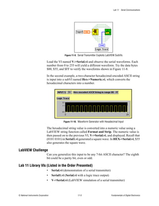
Here are the key gates covered in this lab:
- AND gate
- OR gate
- XOR (exclusive OR) gate
- NOT gate
- NAND gate (NOT AND gate)
- NOR gate (NOT OR gate)
- NXOR gate (NOT exclusive OR gate)
Lab 1 Library VIs
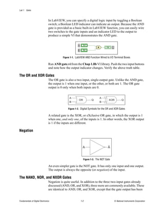
The Lab 1 VI library contains the following VIs:
- AND gate.vi - 3 AND.vi
- OR gate.vi - XOR from NAND.vi
- Truth table.vi - E-switch.vi
These VIs demonstrate the basic gates and some of their applications like
masking and building gates from NAND gates. Feel free

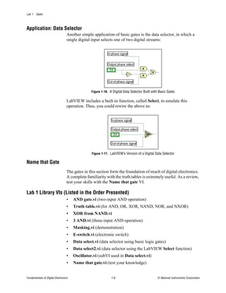
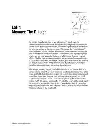
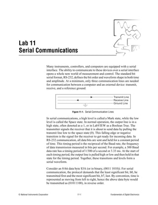
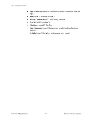
![Lab 4 Memory: The D-Latch
PreSet
D Q Q Set Clr Q Q
0 0 1 0 0 disallowed
D Q
1 1 0 0 1 1 0
1 0 0 1
Clock Q clocked logic 1 1 clocked
Clr
Figure 4-1. D-Latch Symbol and Truth Tables
Data present on the input D is passed to the outputs Q and Q when the clock
is asserted. The truth table for an edge-triggered D-latch is shown to the
right of the schematic symbol. Some D-latches also have Preset and Clear
inputs that allow the output to be set HI or LO independent of the clock
signal. In normal operation, these two inputs are pulled high so as not to
interfere with the clocked logic. However, the outputs Q and Q can be
initialized to a known state, using the Preset and Clear inputs when the
clocked logic is not active.
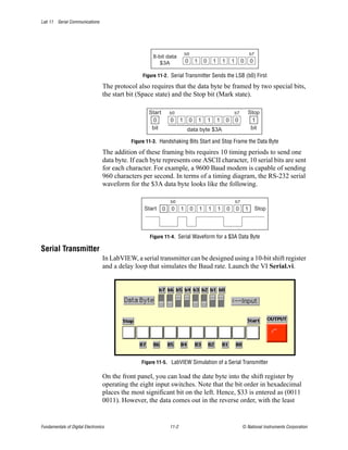
Figure 4-2. LabVIEW Simulation of a D-Latch
In LabVIEW, you can simulate the D-latch with a shift register added to a
While Loop. The up-arrow block is the D input, and the down-arrow block
is the output Q. The complement is formed with an inverter tied to the Q
output. The clock input is analogous with the loop index [i]. You can use a
Boolean constant outside the loop to preset or clear the output. D Latch.vi,
shown above, uses an unwired conditional terminal to ensure that the
D-latch executes only once when it is called.
Shift Registers
In digital electronics, a shift register is a cascade of 1-bit memories in which
each bit is updated on a clock transition by copying the state of its neighbor.
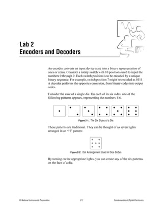
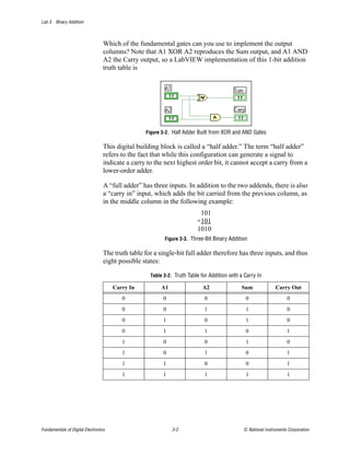
Fundamentals of Digital Electronics 4-2 © National Instruments Corporation](https://image.slidesharecdn.com/digitalece-100930132604-phpapp01/85/Digital-ece-26-320.jpg)
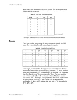
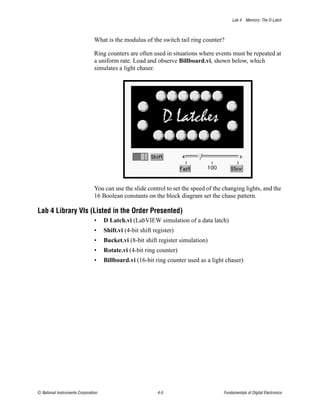
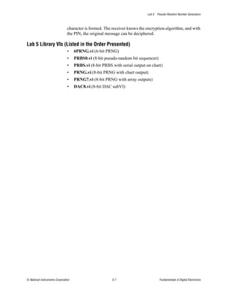
![Lab 4 Memory: The D-Latch
Q1 Q2 Q3 Q4
HI or LO D Q D Q D Q D Q
Q Q Q Q
Clock
Figure 4-3. 4-Bit Shift Register
The bits at the ends have only one neighbor. The input bit D is “fed” from
an external source (HI or LO), and the output Q4 spills off the other end of
the shift register. Here is an example of a 4-bit shift register whose initial
output state is [0000] and input is [1]:
Clock Cycle Q1 Q2 Q3 Q4
n 0 0 0 0
n+1 1 0 0 0
n+2 1 1 0 0
n+3 1 1 1 0
n+4 1 1 1 1
To “cascade” D-latches as above in LabVIEW, additional elements are
added to the D-latch shift register. For example, here is the 4-bit register.
Shift.vi executes the above sequence.
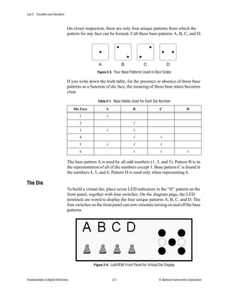
Figure 4-4. Block Diagram for an 8-Bit Shift Register
It is a simple matter to add additional elements to simulate larger width shift
registers. The following VI, Bucket.vi, simulates a “bucket brigade” where
a single bit is introduced on the input D and propagates down the line, where
it spills out and is lost after passing Q8.
© National Instruments Corporation 4-3 Fundamentals of Digital Electronics](https://image.slidesharecdn.com/digitalece-100930132604-phpapp01/85/Digital-ece-27-320.jpg)
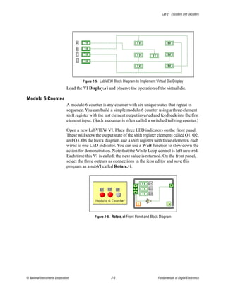
![Lab 4 Memory: The D-Latch
Figure 4-5. Front Panel of an 8-Bit Shift Register Simulation
LabVIEW Challenge
Design a VI in which after the “bucket” passes the last bit, a new bucket is
added at the input D, and the process continues forever.
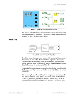
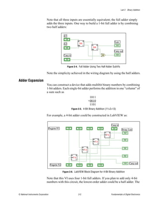
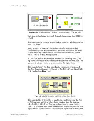
Ring Counters
If the output of a shift register is “fed” back into the input, after n clock
cycles, the parallel output eventually will repeat and the shift register now
becomes a counter. The name ring counter comes from looping the last
output bit back into the input. A simple 4-bit ring counter takes the last
output, Q4, and loops it back directly to the input of the shift register, D.
Q1 Q2 Q3 Q4
D Q D Q D Q D Q
Q Q Q Q
Clock
Figure 4-6. 4-Bit Ring Counter Using Integrated Circuit Chips
In the above case, the outputs have been preset to [0110]. Load and run
Rotate.vi. Observe how the outputs cycle from [0110] to [0011] to [1001]
to [1100] and back to [0110]. It takes four clock cycles, hence this counter
is a modulo 4 ring counter. In a special case where these four outputs are
passed to the current drivers of a stepping motor, each change in output
pattern results in the stepping motor advancing one step. A stepping motor
with a 400-step resolution would then rotate 0.9 degrees each time the
counter is called. A slight variation of the ring counter is the switched tail
ring counter. In this case, the complement output Q of the last stage is fed
back into the input. Modify Rotate.vi to make this change and save it as
Switch Tail Ring Counter.vi.
Fundamentals of Digital Electronics 4-4 © National Instruments Corporation](https://image.slidesharecdn.com/digitalece-100930132604-phpapp01/85/Digital-ece-28-320.jpg)

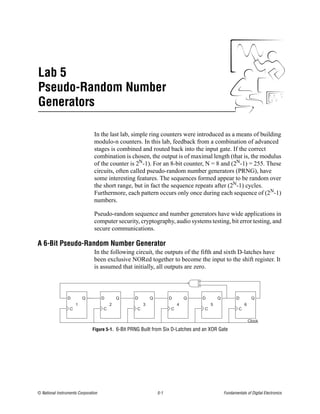
![Lab 5 Pseudo-Random Number Generators
Figure 5-3. LabVIEW Simulation of an 8-Bit PRNG
As in the previous example, the parallel output can be observed on eight
LED indicators. In addition, a pseudo-random sequence of ones and zeros is
produced at Serial Out.
Many digital circuits need to be tested with all combinations of ones and
zeros. A “random” Boolean sequence of ones and zeros at [Serial Out]
provides this feature. In this configuration, the circuit is called a
pseudo-random bit sequencer, PRBS. On the front panel of the above VI,
PRBS0.vi, you can view the Boolean sequence [Serial Out] on an LED
indicator.
Figure 5-4. Front Panel of the 8-Bit PRBS
© National Instruments Corporation 5-3 Fundamentals of Digital Electronics](https://image.slidesharecdn.com/digitalece-100930132604-phpapp01/85/Digital-ece-33-320.jpg)

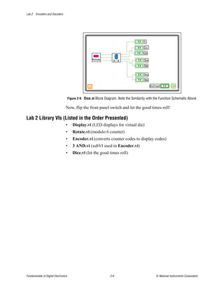
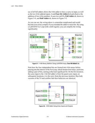
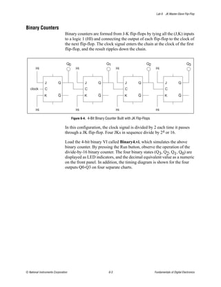
![Lab 6
JK Master-Slave Flip-Flop
One of the most important clocked logic devices is the master-slave JK
flip-flop. Unlike the D-latch, which has memory only until another clock
pulse comes along, the JK flip-flop has true memory. When the J and K
inputs are low, the state of the outputs Q and Q are unchanged on clocking.
Thus, information can be placed onto the output bit and held until requested
at a future time. The output Q can be clocked low or high by setting the (J,K)
inputs to (0,1) or (1,0), respectively. In fact, placing an inverter between J
and K inputs results in a D-latch circuit. The schematic diagram for the JK
flip-flop and its truth table is shown below. Note that the JK flip-flop can
also be Set or Reset with direct logic inputs.
Set
clock J K Q Q Set Clr Q Q
0 0 no change 0 0 disallowed
J Q
0 1 0 1 0 1 1 0
clk
1 0 1 0 1 0 0 1
K Q 1 1 toggle 1 1 clocked
clocked logic direct logic
Clr
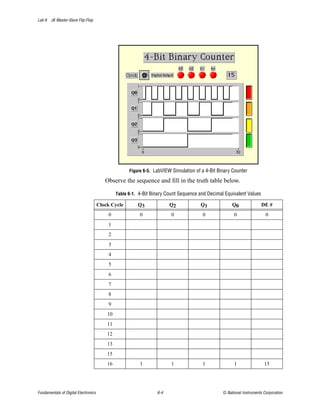
Figure 6-1. JK Flip-Flop Logic Symbol and Truth Tables
The first entry of the clocked truth table is the memory state, while the next
two combinations are the latched states. What is new with the JK flip-flop
is the fourth combination (1,1), which produces a toggle state. On clocking,
the output changes from [1-->0] if 1 or [0-->1] if 0. This complement
function is often referred to as bit toggling, and the resulting flip-flop (J and
K inputs pulled HI) is called a T flip-flop. Because only one toggle occurs
per output cycle, it takes two clock cycles to return the output state to its
initial state. Load Binary1.vi and observe the operation of the T-flip-flop on
clocking.
© National Instruments Corporation 6-1 Fundamentals of Digital Electronics](https://image.slidesharecdn.com/digitalece-100930132604-phpapp01/85/Digital-ece-39-320.jpg)
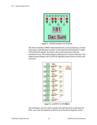
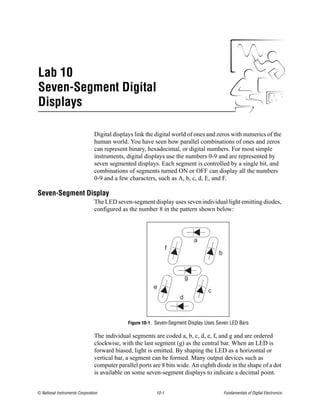
![Lab 10 Seven-Segment Digital Displays
On the block diagram, a 4-bit digital-to-analog converter completes the
operation.
Figure 10-4. LabVIEW VI for a 4-Bit Digital-to Analog Converter
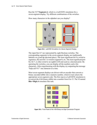
The next step is to convert the digit(s) 0 to 15 into the appropriate
seven-segment display. For the numbers 10 to 15, a single hexadecimal
character [A to F] is used. In Encoder Hex.vi, multiple case statements are
used to provide the encoder function. The Case terminal ? is wired to a
numeric control formatted to select a single integer character. The number 0
outputs the seven-segment code for zero, number 1 outputs the code for 1,
etc., all the way to F. The Boolean constants inside each Case statement are
initialized to generate the correct seven-segment code.
Figure 10-5. LabVIEW VI for Numeric-to-Seven-Segment Display
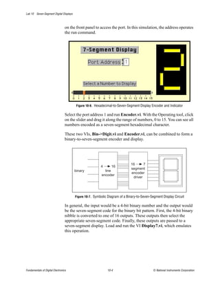
The hexadecimal number inside the square box is the hexadecimal
representation for the 8-bit pattern necessary to represent the number, #n.
Each port has a unique address that must be selected before data can be
written to or read from the real world. The correct address must be entered
© National Instruments Corporation 10-3 Fundamentals of Digital Electronics](https://image.slidesharecdn.com/digitalece-100930132604-phpapp01/85/Digital-ece-65-320.jpg)

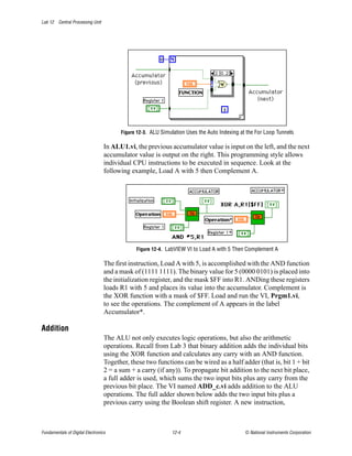
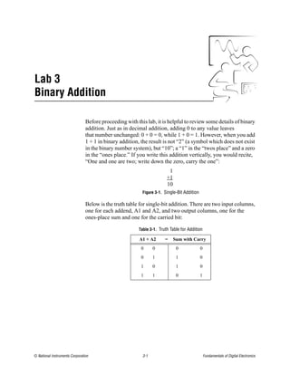
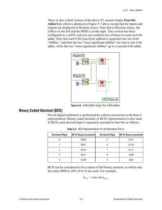
![Lab 12 Central Processing Unit
Operation of the Arithmetic and Logic Unit
The arithmetic and logic unit (ALU) is a set of programmable two-input
logic gates that operate on parallel bit data of width 4, 8, 16, or 32 bits. This
lab will focus on 8-bit CPUs. The input registers will be called Register 1
and Register 2, and for simplicity the results of an operation will be placed
in a third register called Output. The type of instruction (AND, OR, or XOR)
is selected from the instruction mnemonic such as AND R1,R2.
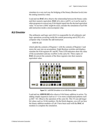
Figure 12-1. LabVIEW Simulation of an Arithmetic and Logic Unit
In the LabVIEW simulation, ALU0.vi, the registers R1 and R2 are
represented by 1D arrays having Boolean controls for inputs. The output
register is a Boolean array of indicators. The function (AND, OR, or XOR)
is selected with the slide bar control. Data is entered into the input registers
by clicking on the bar below each bit. Running the program executes the
selected logic function.
The following are some elementary CPU operations.
What operation does AND R1[$00], R2[$XX]
OR R1[$FF], R2[$XX]
or XOR R1[$55], R2[$FF] represent?
In each case, the data to be entered is included inside the [ ] brackets as a
hexadecimal number such as $F3. Here, X is used to indicate any
hexadecimal character. Investigate the above operations using ALU0.vi.
The AND operation resets the output register to all zeroes, hence this
operation is equivalent to CLEAR OUTPUT. The OR operation sets all bits
high in the output register, hence this operation is equivalent to SET
OUTPUT. The third operation inverts the bits in R1, hence this operation is
equivalent to COMPLEMENT Register 1.
Fundamentals of Digital Electronics 12-2 © National Instruments Corporation](https://image.slidesharecdn.com/digitalece-100930132604-phpapp01/85/Digital-ece-76-320.jpg)
![Lab 12 Central Processing Unit
Consider the operation “Load the Output Register with the contents
contained in R1.” In a text-based programming language, this operation
might read “Output = Register 1.” Set R1 in ALU0.vi to some known value
and execute the operation AND R1,R2[$FF].
Another interesting combination, XOR R1,R1, provides another common
task, CLEAR R1. It should now be clear from these few examples that many
CPU operations that have specific meaning within a software context are
executed within the CPU using the basic gates introduced in Lab 1.
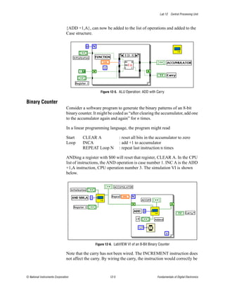
The Accumulator
In ALU0.vi, CPU operations are executed by stripping off one bit at a time
using the Index Array function, then executing the ALU operation on that
bit. The result is passed on to the output array at the same index with
Replace Array Element. After eight loops, each bit (0...7) has passed
through the ALU, and the CPU operation is complete.
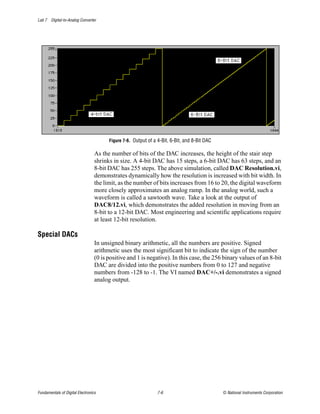
Figure 12-2. LabVIEW VI to Simulate the Operation of an 8-Bit ALU
In LabVIEW, it is not necessary to strip off each bit, as this task can be done
automatically by disabling indexing at the For Loop tunnels. Array data
paths are thick lines, but become thin lines for a single data path inside the
loop. Study carefully the following example, which uses this LabVIEW
feature.
In many CPUs, the second input register, R2, is connected to the output
register so that the output becomes the input for the next operation. This
structure provides a much-simplified CPU structure, but more importantly,
the output register automatically becomes an accumulator.
© National Instruments Corporation 12-3 Fundamentals of Digital Electronics](https://image.slidesharecdn.com/digitalece-100930132604-phpapp01/85/Digital-ece-77-320.jpg)